Galaxy s4 motherboard diagram Samsung galaxy s4 teardown S4 samsung galaxy teardown mobile board s3 motherboard schematics i9505 i9500 techinsights evolution device technology front gt mạch phone choose
Samsung Galaxy S3 i9300 Schematics
Galaxy samsung s3 diagrams manual references faq videos Samsung galaxy s3 i9300 schematics Samsung galaxy teardown circuit splitting technologies mm ii latest global main board
I9300 schematics tháng sáu pham comments
Schematics i9300 j2 sơ i9100 tải về đồ mạchSamsung schematics & manual Samsung galaxy s7 schematics mobile manual edge phone diagram circuit pdf service android inside schematic motherboard diagrams teardown parts mainMotherboard pcb 4g mainboard android broadcom 3g wi.
Samsung galaxy s3 gt-i9300 speaker problem3/1/11 ~ mobile phone repair guides Galaxy s ii teardown – splitting 8.9 mm of the latest samsung[download 43+] samsung i9500 schematic diagram download.

Introducing samsung galaxy s5
Shenzhen professional circuit board assembler samsung galaxy s3 pcbSchematic diagrams samsung galaxy s5 sm g900f Schematic galaxy g900fBoard circuit pcb samsung professional shenzhen assembler galaxy s3.
Galaxy s schematicsMotherboard diagram galaxy s4 easily carefully pull pop should S3 samsung galaxy speaker i9300 problem gtS4 wiring.

Samsung schematic diagram schematics diagrams
Download samsung schematic diagramS4 screen lcd i9505 jumper galaxy samsung possible Pcb layout 4gSamsung galaxy schematics s5 s6 mobile.
[download 43+] samsung i9500 schematic diagram downloadGakaxy s4 i9505 lcd black screen Samsung glaxy-s3 i9300 charging problemSamsung galaxy s 4g pcb board components layout ~ mobile phone repair.

Charging samsung s3 i9300 glaxy problem
Inside the samsung galaxy s iii: quad-core drives galaxial screenSamsung galaxy s3 i9300 schematics Nand dibalik rahasia inside exynos cnet.
.

Introducing SAMSUNG Galaxy S5
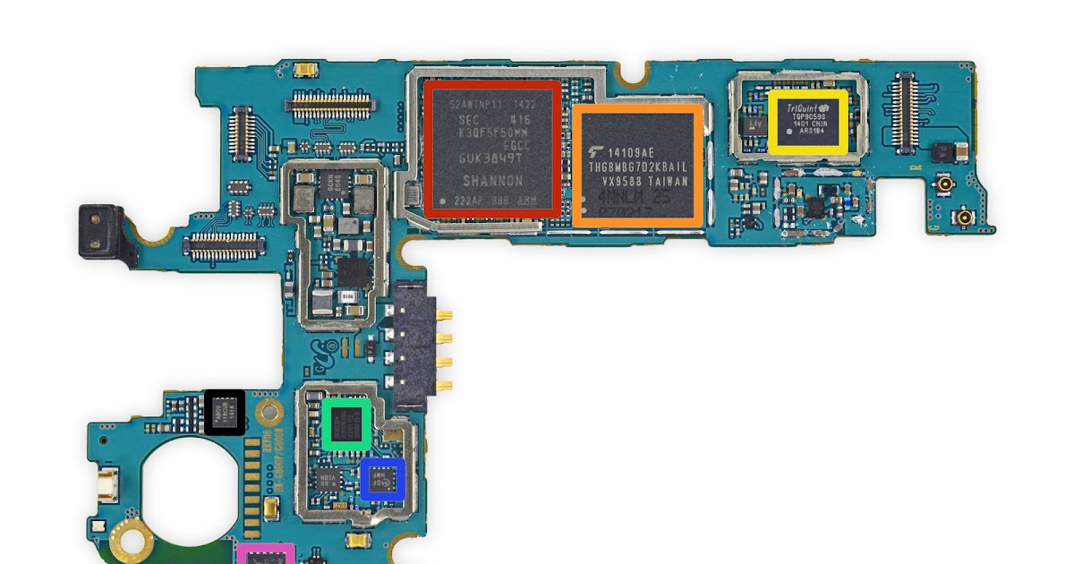
Schematic Diagrams Samsung Galaxy S5 SM G900F - Mobite
![[Download 43+] Samsung I9500 Schematic Diagram Download](https://i2.wp.com/lh5.googleusercontent.com/proxy/BRZzM0_qlryPkDyvoFbdHxT51XaZ3Js6DxuTYWMMWa6p_9B4JgYDgpqZYqbxK0C7o7T-jJUxfQtc3ASGYE6vgoXNGkaZ6aSjTtnTZMMXJwM0TZqo75t_uIad44nFEROIYA=s0-d)
[Download 43+] Samsung I9500 Schematic Diagram Download

Diagrams - Samsung Galaxy s3

Gakaxy S4 i9505 LCD Black Screen - GSM-Forum

Samsung Schematics & Manual - All Keypad & Android Mobile circuit

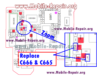
Samsung Galaxy S3 i9300 Schematics

3/1/11 ~ Mobile Phone Repair Guides